Final Year Project: Week 6
1) DE2 board using the LED and switch
- The DE2 board provides four pushbutton switches. Each of these switches is debounced using a Schmitt Trigger circuit. The four outputs called KEY0 until KEY3 of the Schmitt Trigger device are connected directly to the Cyclone II FPGA. Each switch provides a high logic level (3.3 volts) when it is not pressed, and provides a low logic level (0volts) when depressed. Since the pushbutton switches are debounced, they are appropriate for use as clock or reset inputs in a circuit.There are also 18 toggle switches (sliders) on the DE2 board. These switches are not debounced, and are intended for use as level-sensitive data inputs to a circuit. Each switch is connected directly to a pin on the Cyclone II FPGA. When a switch is in the DOWN position (closest to the edge of the board) it provides a low logic level (0 volts) to the FPGA, and when the switch is in the UP position it provides a high logic level (3.3 volts).A schematic diagram that shows the push button and toggle switches is shown as below:

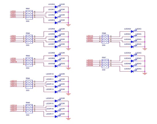
- There are 27 user-controllable LEDs on the DE2 board. Eighteen red LEDs are situated above the18 toggle switches, and eight green LEDs are found above the pushbutton switches (the 9th green LED is in the middle of the 7-segment displays). Each LED is driven directly by a pin on the Cyclone II FPGA, driving its associated pin to a high logic level turns the LED on, and driving the pin low turns it off. A schematic diagram that shows the LED circuitry shown as below:
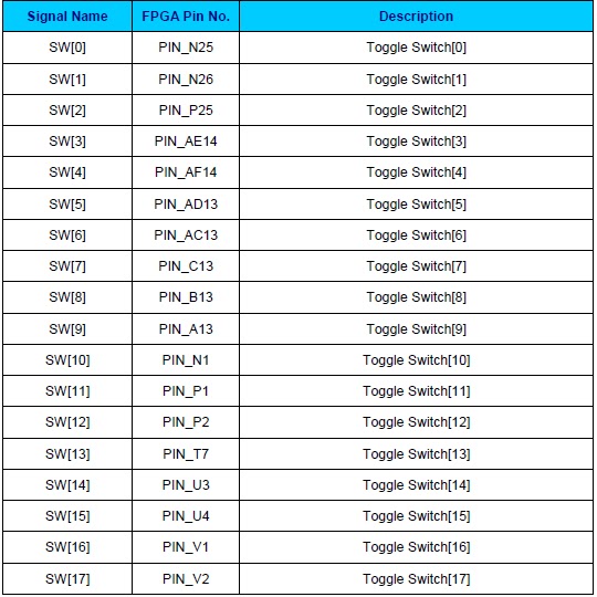
- Pin Assignments; Pin assignments are made by using the Assignment Editor in Quartus II Software. It can get from DE2 User Manual.The table of Pin assignment for the toggle switches,push button switches and LEDs shown as below:
 |
| Pin assignments for the toggle switches |
 |
| Pin assignments for the LEDs. |
 |
| Pin assignments for the push button switches | |
2) Test DE2 board using the LED and switch
- Created and testing the 16 bit up counter with active low preset and clear function using LEDs and toggle switch as a input/output.Verilog HDL coding and pin assignment for 16 bit up counter with active low preset and clear function shown as below:
 |
| Verilog HDL coding |
 |
| RTL viewer |
 |
| Pin Assignments |
 |
| Output at DE2 Board |


No comments:
Post a Comment