Final Year Project: Week 7
1) DE2 board using the 7- segments Display
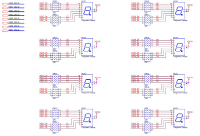
- The DE2 Board has eight 7-segment displays. These displays are arranged into two pairs and a group of four, with the intent of displaying numbers of various sizes. As indicated in the schematic in Figure A, the seven segments are connected to pins on the Cyclone II FPGA. Applying a low logic level to a segment causes it to light up, and applying a high logic level turns it off. Each segment in a display is identified by an index from 0 to 6, with the positions given in Figure B. Note that the dot in each display is unconnected and cannot be used. Table C shows the assignments of FPGA pins to the 7-segment displays.
 |
| Figure A:Schematic diagram of the 7-segment display |
 |
| Figure B:Position and index of each segment in a 7-segment display |
 |
 |
 | |||||
| Figure C:Pin assignments for the 7-segment displays |
2) Test DE2 board using the 7- segments Display
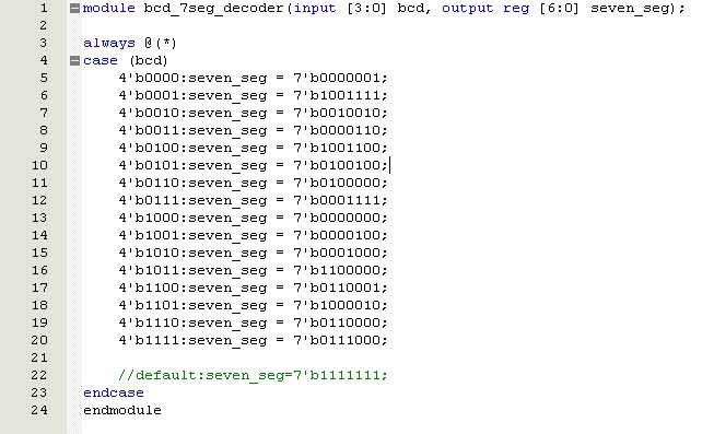
- Created and testing the BCD to 7- segments decoder using 7-segment displays as output.Verilog HDL coding and pin assignment for BCD to 7- segments decoder shown as below:
 |
| Verilog HDL coding for BCD to 7- segments decoder |
 |
| RTL viewer |
 |
| Pin Assignments |
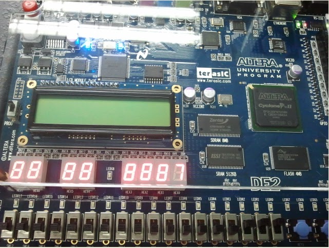 |
| Output at DE2 Board |
No comments:
Post a Comment