Project Summary:

The purpose of this project is to gain a theoretical knowledge about FPGA, VGA and do some research on how to use ALTERA DE 2 BOARD also do some research on how to write a coding using Verilog HDL and researcher will expected to display an image in the VGA through ALTERA DE2 board.

Sunday 26 February 2012

Final Year Project: Week 6


1) DE2 board using the LED and switch

  •  The DE2 board provides four pushbutton switches. Each of these switches is debounced using a Schmitt Trigger circuit. The four outputs called KEY0 until KEY3 of the Schmitt Trigger device are connected directly to the Cyclone II FPGA. Each switch provides a high logic level (3.3 volts) when it is not pressed, and provides a low logic level (0volts) when depressed. Since the pushbutton switches are debounced, they are appropriate for use as clock or reset inputs in a circuit.There are also 18 toggle switches (sliders) on the DE2 board. These switches are not debounced, and are intended for use as level-sensitive data inputs to a circuit. Each switch is connected directly to a pin on the Cyclone II FPGA. When a switch is in the DOWN position (closest to the edge of the board) it provides a low logic level (0 volts) to the FPGA, and when the switch is in the UP position it provides a high logic level (3.3 volts).A schematic diagram that shows the push button and toggle switches is shown as below:


  • There are 27 user-controllable LEDs on the DE2 board. Eighteen red LEDs are situated above the18 toggle switches, and eight green LEDs are found above the pushbutton switches (the 9th green LED is in the middle of the 7-segment displays). Each LED is driven directly by a pin on the Cyclone II FPGA, driving its associated pin to a high logic level turns the LED on, and driving the pin low turns it off.  A schematic diagram that shows the LED circuitry shown as below:


  • Pin Assignments;  Pin assignments are made by using the Assignment Editor in Quartus II Software. It can get from DE2 User Manual.The table of Pin assignment for the toggle switches,push button switches and LEDs shown as below:

Pin assignments for the toggle switches


Pin assignments for the LEDs.
Pin assignments for the push button switches 

2) Test DE2 board using the LED and switch
  • Created and testing the 16 bit up counter with active low preset and clear function  using  LEDs and toggle switch as a input/output.Verilog HDL coding and pin assignment for 16 bit up counter with active low preset and clear function shown as below:

Verilog HDL coding

RTL viewer

Pin Assignments

Output at DE2 Board


Sunday 19 February 2012

Final Year Project: Week 5

1) Attend briefing/meeting with all FYP students on Tuesday16/2/2012 on 3 pm at TTL 1.The agenda is ;
  • Format of FYP report
2) Block Diagram  of the DE2 Board

  •  All connections are made through the Cyclone II FPGA device. It can configure the FPGA to implement any system design.


 3) Overall Structure of the DE2 Control Panel
  • The DE2 Control Panel facility communicates with a circuit that is instantiated in the Cyclone II FPGA. This circuit is specified in Verilog code, which makes it possible for a knowledgeable user to change the functionality of the Control Panel.Each input/output device is controlled by a controller instantiated in the FPGA chip. The communication with the PC is done via the USB Blaster link. A Command Controller circuit interprets the commands received from the PC and performs the appropriate actions. The SDRAM, SRAM, and Flash Memory controllers have three user-selectable asynchronous ports in addition to the Host port that provides a link with the Command Controller. The connection between the VGA DAC Controller and the FPGA memory allows displaying of the default image shown on the left side of the figure, which is stored in an M4K block in the Cyclone II chip. The connection between the Audio DAC Controller and a lookup table in the FPGA is used to produce a test audio signal of 1 kHz.The DE2 Control Panel block diagram shown as below:


Tuesday 14 February 2012

Final Year Project: Week 3 and Week 4

Week3
  
 Introduction to Verilog Hardware Descriptive Language (Verilog HDL)

1.Hardware Description Languages
 
  • A hardware description language is a computer language that is used to describe hardware.
  • Two HDLs are widely used :Verilog HDL and VHDL (Very High Speed Integrated Circuit Hardware Description Language).
  • Schematic design entry can be replaced by writing HDL code that CAD tools understand.
  • CAD tools can verify the HDL codes, and create the circuits automatically from HDL codes.

2. Fact about Verilog

History of Verilog
  • In 1980s, originally developed by Gateway Design Automation.
  • In 1990, was put in public domain.  
  • In 1995, adopted as an IEEE standard 1364-1995  
  • In 2001, an enhanced version, Verilog 2001
 
3.Functions of Verilog HDL
  • Design entry (using schematics or HDL)
  • Simulation and verification of the design
  • Synthesis

4.Design Flow Using Quartus II Verilog HDL and DE2 Board:


 Week 4

1.Create simple design entry using Verilog code to make more understand with Verilog HDL. The Verilog code, design entry , and successful compiling the design circuit shown as below:


Verilog code

Design entry

Successful compiling the design circuit


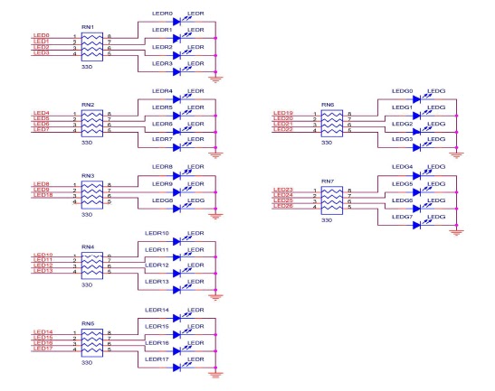
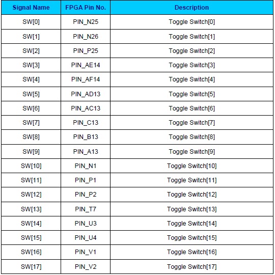
2. Pin Assignment: During the compilation above, the Quartus II Compiler was free to choose any pins on the selected FPGA to serve as inputs and outputs.However, the DE2 board has hardwired connections between the FPGA pins and the other components on the board.I will use two toggle switches, labeled SW1 and SW0, to provide the external inputs, x1 and x2, to the circuit. These switches are connected to the FPGA pins N26 and N25, respectively. I will connect the output f to the green light-emitting diode labeled LEDG0, which is hardwired to the FPGA pin AE22.

The available pins.     

The complete assignment.

3. Performing the simulation: Typically, functional simulation is used to verify the functional correctness of a circuit as it is being designed.The result of timing simulation as shown below:


Result of timing simulation.

4. Programming and Configuring the FPGA Device: The FPGA device must be programmed and configured to implement the designed circuit. The required configuration file is generated by the Quartus II Compiler Assembler module.  The configuration data is transferred from the host computer (which runs the Quartus II software) to the board by means of a cable that connects a USB port on the host computer to the left most USB connector on the board by using  USB-Blaster driver installed. Connected the USB cable and turn on the power supply switch on the board.The programming and configuration task is performed as follows:


The Programmer window.    

The Hardware Setup window.

The Programmer window upon completion of programming

5. Testing the Designed Circuit: Having downloaded the configuration data into the FPGA device, the implemented circuit have tested. The result is the circuit implements is similar the truth table. Its success.