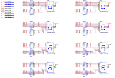
Final Year Project: Week 8
1) DE2 board using the LCD
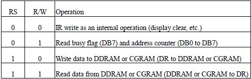
The LCD display Module is built in a LSI controller, the controller has two 8-bit registers, an instruction register (IR) and a data register (DR). The IR stores instruction codes, such as display clear and cursor shift, and address information for display data RAM (DDRAM) and character generator (CGRAM). The IR can only be written from the MPU. The DR temporarily stores data to be written or read from DDRAM or CGRAM. When address information is written into the IR, then data is stored into the DR from DDRAM or CGRAM. By the register selector (RS) signal, these two registers can be selected.
Busy Flag (BF)
When the busy flag is 1, the controller LSI is in the internal operation mode, and the next instruction will not
be accepted. When RS=0 and R/W=1, the busy flag is output to DB7. The next instruction must be written
after ensuring that the busy flag is 0.
When the busy flag is 1, the controller LSI is in the internal operation mode, and the next instruction will not
be accepted. When RS=0 and R/W=1, the busy flag is output to DB7. The next instruction must be written
after ensuring that the busy flag is 0.
Address Counter (AC)
The address counter (AC) assigns addresses to both DDRAM and CGRAM
Display Data RAM (DDRAM)
This DDRAM is used to store the display data represented in 8-bit character codes. Its extended capacity is
80 X 8 bits or 80 characters. Below figure is the relationships between DDRAM addresses and positions on
the liquid crystal display.

Character Generator ROM (CGROM)
The CGROM generate 5x8 dot or 5x10 dot character patterns from 8-bit character codes. See Table 2.
The CGROM generate 5x8 dot or 5x10 dot character patterns from 8-bit character codes. See Table 2.
Character Generator RAM (CGRAM)
In CGRAM, the user can rewrite character by program. For 5x8 dots, eight character patterns can be written, and for 5x10 dots, four character patterns can be written.
Write into DDRAM the character code at the addresses shown as the left column of table 1. To show the
character patterns stored in CGRAM
 |
| Table 1 |
 |
| Table2 |
LCD Timing Characteristic
 |

2) Test DE2 board using LCD
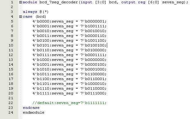
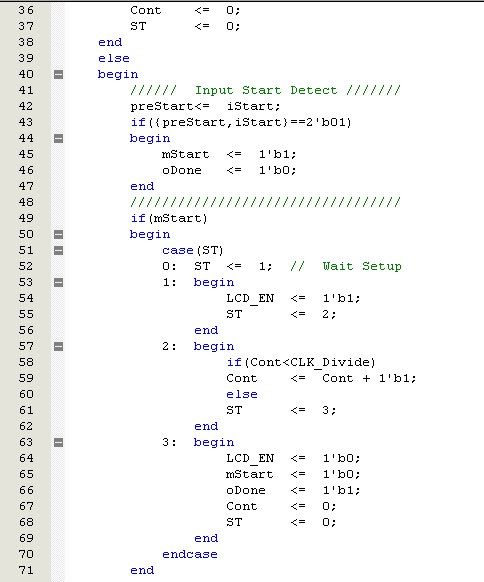
- Created and testing the LCD displays as output. Verilog HDL coding and pin assignment for LCD shown as below:

 | |||||||||||||||||||||
| Verilog HDL coding for LCD Controller |


 |
| RTL viewer |
 |
| Pin Assignments |

 |
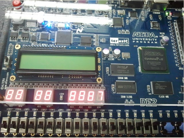
| LCD Output at DE2 Board |